
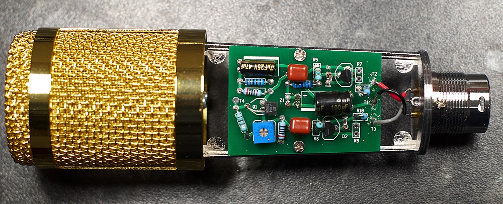
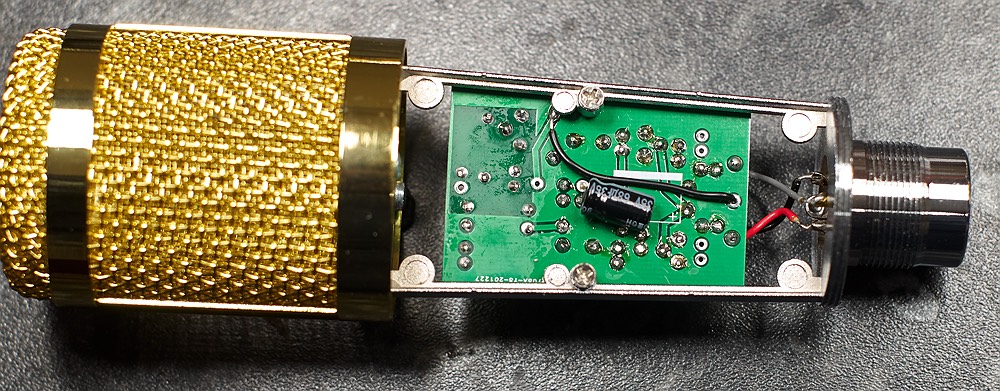
Schoeps style circuit and the PCBs for BM700/800 bodies
Board reference code SCH
Page about the Schoeps circuit and the boards for BM700/800 bodies
email me at parenthetical at this domain with any questions
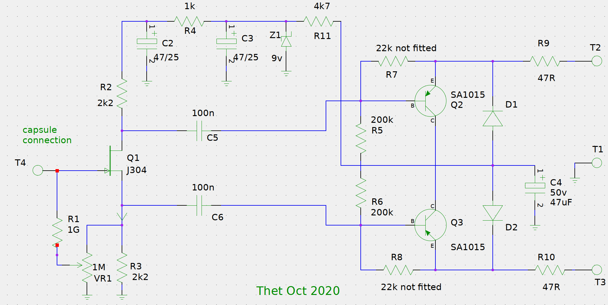
Circuit description and practical tips
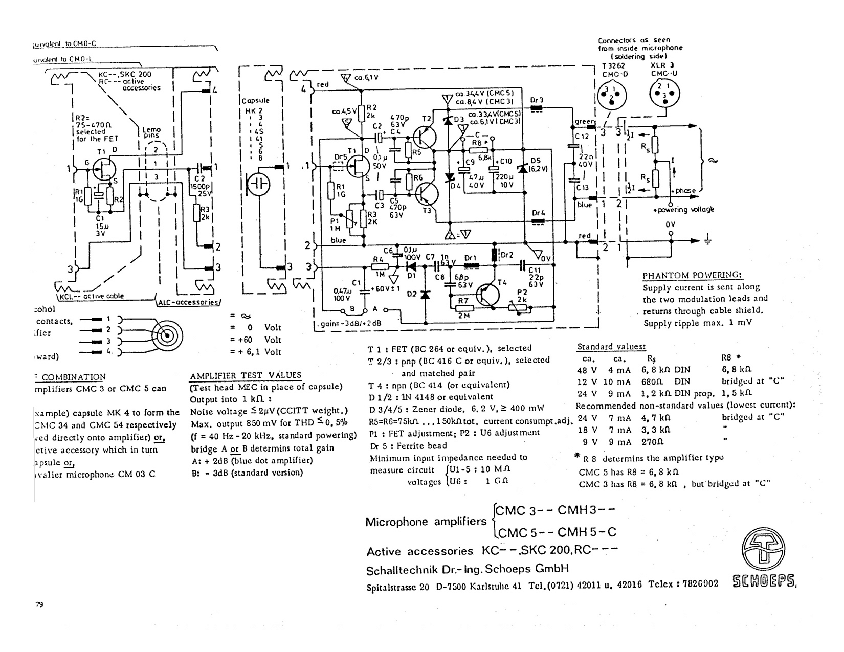
you can see the original Schoeps circuit here:http://www.sdiy.org/oid/mics/Schoeps.gif
This is a lengthy article I wrote mostly so I don't forget what I have learned, and in which I try to explain this circuit in ways different from others I have seen online, and in ways that would have helped me to make sense of it when I was first building these. So if some of this explanation seems an odd way of putting things, that is why!
I will not discuss capsule polarisation here. It is assumed you are using a electret capsule, (without internal fet) or that you know how to apply polarisation to an externally polarised capsule.
Signal flow: Signal enters at T4, goes through the gate of the fet and is split into opposite polarity copies at the drain and source of the fet - these two copies then go through C5 and C6, into the base of the PNP transistors and out the emitter of the transitors to the cable and mic preamp.
Power flow: (seen as conventional flow direction) 48v phantom power enters at T2 and T3, flows through the two PNP transistors from emitter to collector, is stored/stabilised at C4, flows through R11 where is is clamped to 9v by Z1 and filtered by R4 and C2, then flows through the drain resistor R2 then through the fet from drain to source and finally through R3 to ground.
The circuit consists of two sections. Firstly a fet concertina phase splitter and impedance converter followed by two PNP emitter followers used as impedance converters. The signal flows through the fet then through the two PNPs in parallel, but with opposite polarity in each PNP.
For historical reasons, phantom power is high voltage but low current. This was originally to allow capsule polarisation directly from the phantom power source, but it presents a challenge for making a good impedance converter headamp where we would normally prefer more current at lower voltage. The clever thing about this circuit is that the two sections run in series from a power supply point of view. The PNP transistors are stacked on top of the fet so the fet essentially runs on the exhaust current from the output transistors. Since we have loads of voltage but not much current available, this lets us use the same current twice, and we still have plenty of voltage to share between the two sections.
For those like me, who are coming to BJT transistors from valves or fets, I think of the PNP emitter followers like an upside down source follower. (Upside down because a PNP transistor is reverse polarity from a valve or a "normal" NPN transistor). In turn I think of a source follower as a fet version of a valve cathode follower. The emitter resistors are notably missing from the schem, but they are not missing from the circuit! This is because they are the 6.8k resistors that are assumed to be in the mic preamp supplying the phantom power. Any mic preamp that doesn't have these resistors in place is not supplying correct P48 phantom power. The circuit could be built with emitter resistors built in, but we would require an extra power cap, two extra power supply resistors, and two emitter resistors. Since the schoeps circuit was originally designed to fit in a small pencil mic body you can see that it was desirable to keep the parts count down.
Section by section description and part value choices.
The FET
Q1, R1, R2, R3, and VR1 form a concertina phase splitter. Gain approaches 1 for each side of the splitter, if current and transconductance are high enough and R2/R3 are not too low. Seen together the sum of both sides has a gain approaching 2.
I like to use J304 or 2N4416 fets as they sound good to me and usually have a suitable IDSS and transconductance. The fets I use typically have an IDSS between 7 and 12ma. J305 is also a good choice, although some examples might have rather low IDSS and transconductance for this circuit. If you want or need to use a J305 with IDSS at the low end of the range (say below 4ma) then you may want/need to increase the value of R2 and R3 in order to run the phase splitter at lower current. J305s with higher IDSS say above 5ma are usually fine as shown.
Noise is theoretically reduced by keeping R2 and R3 low, however if they are too low for the fet or for the available current then gain will be reduced. 2.2k is fine for the fets I use. R2 and R3 could be as low as 1k or as high as 10k depending on the fet and the desired current. Note however that there is no point in running the fet at low current in this circuit as any unused current will simply be wasted in the zener, and the output transistors will use more than the fet anyway. We are running the fet on the output transistors' exhaust current remember, so there is no point in conserving current in the fet (up to the point at which it uses the same current as both output transistors together).
R1 provides a voltage reference for biasing the fet. VR1 sets this voltage reference by dividing the voltage present at the source. Yes, this results in positive feedback or bootstrapping, but we can ignore that for the purposes of this article.
The fet should be biased by adjusting VR1 until the fet is biased in quarters. By this I mean that the voltage across R2 and R3 should each be 1/4 of the supply voltage at C2. So if we have 8v at C2 then we should have 2v at the fet source and 6v at the fet drain. This ensures that each side of the fet is free to swing equally in both directions.
Noise is reduced by running at lower voltage - but so is headroom - so if you have a low output capsule, say a small diaphragm one, you may want to reduce Z1 to 6.2v - this was the original schoeps value. I use 9v or even 10v for Z1 because I typically use high output large diaphragm condesner capsules with high polarisation voltages which all results in much higher output than the original.
The zener and power supply
The zener Z1 is clamping the supply voltage for the fet to the desired level. R4 and C2 are acting as a low pass filter with a very low corner, to filter out the noise introduced by the zener. C3 will also be filtering the zener a bit, but not as effectively as there is no series resistor forming an RC filter. I am not entirely sure that C3 is necessary, it may be possible to remove it or reduce its value.
Capacitor Choice: I have put 47uF 25v for C2 and C3 as that is what I use. However you can use any voltage larger than the zener voltage, and make them as large capacitance as you can fit. I use Panasonic FR, FM, or FC caps for electrolytics as they have very low ESR and sound great.
We use the zener for convenience because it allows us to set the supply voltage for the fet independently of its exact current consumption. Any current available at C4 that is not used by the fet is then wasted in R11 and Z1. It is possible to eliminate the zener by careful balancing of the current used in the fet and the BJTs so they match at the desired bias point for each, but this is much more effort than using the zener. In the unlikely event that the fet tries to use more current than is available at C4 and further reduced by R11 then the fet supply voltage at C2 will drop below the zener voltage. If this happens then R11 can be reduced, although checking that bias points are all optimal would also be in order.
The output transistors
The inputs (base) of Q2 and Q3 are coupled to the outputs of the concertina splitter through C5 and C6. The input impedance of the Q2/3 is largely determined by the value of R5/6 which also sets the bias for the output transistors.
If we were designing for neutral / flat response without phase shift then C5/6 should be as large a practical. 100nF will give full range bass response when considered purely in terms of corner frequency, but will introduce a low frequency phase shift that extends into the audible range. Increasing C5/6 may be desirable in some uses to avoid this, but the difference is subtle, and depnds on the rest of your signal chain. Conversely if you want a built in LF rolloff you can reduce C5/C6 to make a high pass filter.
In most practical situations for most users having a subsonic rolloff (to avoid rumble and LF noise eating headroom) may be more desirable than phase neutral response. In this case the caps should be kept to 100nF or so.
It is possible to obtain film caps that fit - in values up to 1uF. These should be high quality film caps. I use panasonic ECQV 50v as they sound good to me, and are small for their value. Wima FKP2 would also be a good choice sonically, but they are quite a bit larger and the larger values may be difficult to fit.
If the transistors are perfectly matched then the point where the collectors meet should have a steady voltage, however in practice there will be some imbalance. C4 provides a stable DC point to absorb any imbalance and to provide the first stage of the power supply for the fet. The operating voltage across C4 depends on the transistor bias, but is usually around 32v. It can be higher and there can be higher surge voltages on switch-on so it's best to stick to 50v caps here. I originally specified 100uF becaue I feel it is important that this point in the circuit is as stable as posible, however 47uF is probably plenty. I haven't worked out what size is actually needed.
Changing the value of R5/6 is the main way to bias the output transistors for the right amount of headroom and current draw. I have specified R5/6 as 200k because that suits the high Hfe SA1015 transistors that I have. The original value was 100k, and that may suit transistors with lower current gain.
The collector to emitter voltage (Vce) is a good approximate guide to the headroom in the output transistors. The maximum clean signal swing will be a little less than twice Vce. However the output transistors are biased warm. They have loads of headroom on the 48v side, and the collector side will saturate/clip very gradually.
The fet and the output transistors should be biased to run with about the same headroom in each so Vce at the BJT should be set about the same as the voltage from the fet source to ground.
Increasing the value of R5/6 will bias the output transistors cooler, reduce current draw and increase headroom. I have had 100k CB resistors give Vce of 2v with some transistors and only 1.2v in others.
R7 and R8 are usually not fitted and not required. However if you find that you need very large values of R5/6 to get enough headroom from the transistors then fitting R7/8 will bias the transistors cooler, and increase Vce and headroom. The smaller the value of R7/8 the cooler the transistors will run. You can also use these pcb positions to fit 1N4148 diodes to protect the b-e junctions directly - more on that in the future.
Reducing the current through the output transistors will increase headroom, up to the point where the emitter voltage is halfway between the collector voltage and the 48v supply. It will also reduce the current draw, which has the effects of: 1. raising the voltage at the XLR (relevant if you want to use this for capsule polarisation), 2. increasing the output impedance a little. 3. reducing the current available to the fet.
Diodes D1 and D2 are there to protect the transistors - more on this later, it's an issue that merits its own article. They are traditionally 6.2v zeners although I have not managed to find any fault situation where the zener function is required or beneficial. 1N4148 can also be used.
Steps to set correct headroom for the whole circuit:
* Decide how much clean signal the circuit must be able to handle, and then add a little. Lets say we want to handle 2.5v peak to peak from the capsule, so we'll round that up to 3v. (What is max output for a LDC at 60v polarisation? Would be useful to mention here, and I will do so when I have a figure.)
* Multiply that by 2, that's your fet supply voltage 6v.
* Bias the fet so that it has 1/4 of that dropped across each resistor, so source is 1.5v, drain is 4.5v.
* Set the BJT's Vce to 1.5v by selecting the C-B resistor to give that value. Larger resistors will increase Vce. Don't just blindly use the values on the schematic as they may be wrong (or at least suboptimal) for your particular fet voltage and BJT gain.
I generally use 9v fet supply for 2v+ at the source, and near 4v peak to peak handling, because I like headroom.